

Researchers at Osaka University have introduced an innovative technology that can reduce the power consumption of modern storage devices.
Among the current mainstream memory technologies, DRAM, although fast, has high power consumption, low capacity, high cost, and cannot retain data after power loss, limiting its use scenarios; NAND Flash has low read-write speed, and its storage density is significantly constrained by process technology.
In order to overcome the limitations of traditional memory devices such as DRAM and NAND Flash, the barriers in memory technology are being continually broken, and new types of memory technology are starting to enter the public’s view.
In recent years, various types of memory devices have emerged in computing equipment, aimed at overcoming the limitations of traditional Random Access Memory (RAM). Magnetoresistive RAM (MRAM) is one such memory type that has multiple advantages over traditional RAM, including non-volatility, high speed, increased storage capacity, and enhanced durability. Although MRAM devices have made significant improvements, reducing energy consumption during data write operations remains a key challenge.
Researchers at Osaka University recently published a study in the journal Advanced Science, proposing a new low-energy data write technology for MRAM devices. Compared to current current-based methods, this technology enables an electric-field-based write scheme with lower energy consumption, potentially offering an alternative to traditional RAM.
Conventional Dynamic RAM (DRAM) devices have basic storage units composed of transistors and capacitors. However, the stored data is volatile, meaning energy input is required to retain the data. In contrast, MRAM uses magnetic states (such as magnetization direction) to write and store data, achieving non-volatile data storage.
“Because MRAM devices rely on the non-volatile magnetization state in capacitors rather than the volatile charge state, they consume less power in standby mode and are a promising alternative to DRAM,” explained the lead author of the study, Takamasa Usami.
Current MRAM devices generally require current to switch the magnetization vector of the magnetic tunnel junction, similar to how DRAM devices switch the charge state of capacitors. However, a large current is needed during the writing process to switch the magnetization vector, which inevitably generates Joule heating and leads to energy consumption.
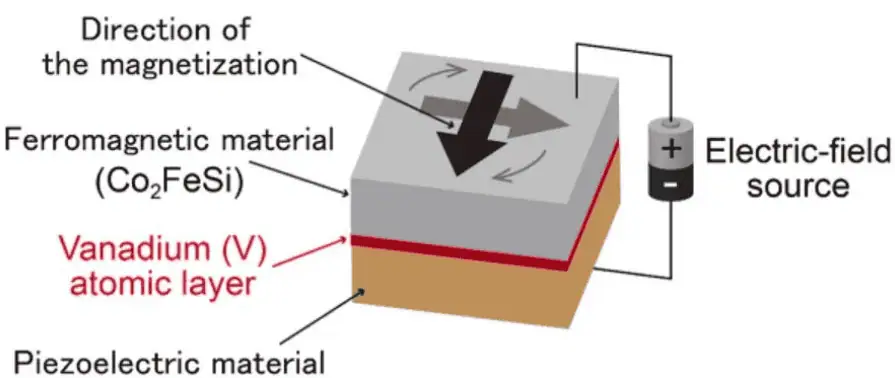
To address this issue, the researchers developed a new component for controlling the electric field in MRAM devices. The key technology is a multiferroic heterostructure, whose magnetization vector can be switched by an electric field (Figure 1). The response of the heterostructure to the electric field can essentially be characterized by the inverse magnetoelectric (CME) coupling coefficient, with larger values indicating stronger magnetization response.
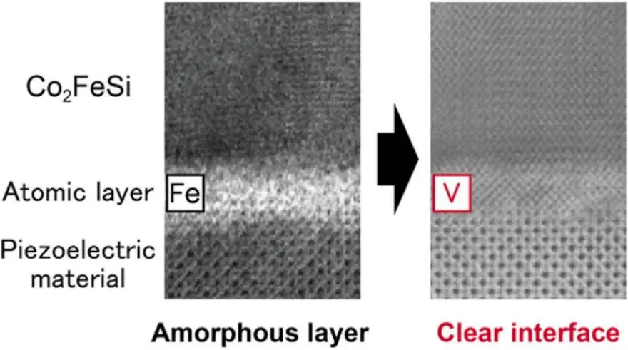
The researchers had previously reported a multiferroic heterostructure with a CME coupling coefficient exceeding 10-5 s/m. However, structural fluctuations in the ferromagnetic layer (Co2FeSi) made it difficult to achieve the required magnetic anisotropy, hindering reliable electric field operation. To improve the stability of this structure, the researchers developed a new technology in which an ultra-thin vanadium layer is inserted between the ferromagnetic and piezoelectric layers. As shown in Figure 2, inserting the vanadium layer creates a clear interface, making it possible to reliably control the magnetic anisotropy in the Co2FeSi layer. Additionally, the CME effect achieved a value greater than that of similar devices without the vanadium layer.
The researchers also demonstrated that by altering the scanning operation of the electric field, two distinct magnetic states can be reliably achieved under zero electric field. This means that non-volatile binary states can be deliberately realized under zero electric field.
“By precisely controlling the multiferroic heterostructure, we can meet two key requirements for practical magnetoelectric (ME)-MRAM devices: non-volatile binary states with zero electric field and a large CME effect,” said senior author Kohei Hamaya.
This spintronic device research may ultimately be realized in practical MRAM devices, enabling manufacturers to develop ME-MRAM, a low-power write technology suitable for a wide range of applications requiring persistent and secure memory.
It is noteworthy that the current emerging memory market is primarily focused on low-latency memory and persistent memory, and does not yet have the capability to replace DRAM/NAND Flash. However, in the era of explosive data growth, new memory technologies, with their exceptional characteristics such as ultra-high performance, long lifespan, reliability, and high-temperature resistance, are expected to become a new choice in the memory field.
Currently, traditional memory devices still occupy the vast majority of the market share, but with the arrival of the 5G era, the development of the Internet of Things, artificial intelligence, smart cities, and other application markets, along with diverse demands for memory and factors like price fluctuations in the traditional memory market, new memory devices will play an increasingly important role in the market.
Related:

Disclaimer:
- This channel does not make any representations or warranties regarding the availability, accuracy, timeliness, effectiveness, or completeness of any information posted. It hereby disclaims any liability or consequences arising from the use of the information.
- This channel is non-commercial and non-profit. The re-posted content does not signify endorsement of its views or responsibility for its authenticity. It does not intend to constitute any other guidance. This channel is not liable for any inaccuracies or errors in the re-posted or published information, directly or indirectly.
- Some data, materials, text, images, etc., used in this channel are sourced from the internet, and all reposts are duly credited to their sources. If you discover any work that infringes on your intellectual property rights or personal legal interests, please contact us, and we will promptly modify or remove it.