
At the end of last year, the ban on HBM struck the domestic semiconductor industry like a heavy blow, triggering considerable disruption.
In December last year, the U.S. Department of Commerce’s Bureau of Industry and Security (BIS) officially revised the Export Administration Regulations (EAR), imposing stricter export controls on HBM and a series of semiconductor manufacturing equipment and software tools, and added 140 Chinese entities to the export control list. In particular, HBM products with a “memory bandwidth density” exceeding 2GB/s/mm²—essentially covering all currently mass-produced models—were targeted, directly cutting off a crucial supply chain for Chinese companies in the advanced memory field.
At the time, many believed this restriction would place immense pressure on the domestic semiconductor industry, especially for the AI sector, which heavily depends on HBM. Without access to HBM, a wider gap with overseas competitors seemed inevitable.
It was precisely under such heavy constraints that domestic memory manufacturers began seeking high-bandwidth memory opportunities beyond HBM.
In reality, AI applications are not entirely dependent on HBM. As of now, many NVIDIA and AMD GPUs still use GDDR memory, which can deliver bandwidths of 800–960GB/s. Although this is far below the rate of HBM 3E, such bandwidth is already sufficient for smaller-scale inference of large language models.
And if GDDR isn’t enough, SRAM and system-level scaling have also proven to be effective alternatives to HBM. Companies like Cerebras and Groq have demonstrated this by allocating large amounts of SRAM to each chip and using high-speed interconnects or wafer-scale packaging to link the chips together, achieving extremely high AI inference throughput—sometimes even surpassing systems using standalone HBM memory.
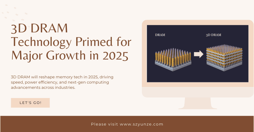
In China, 3D DRAM has become a focal point for some memory manufacturers.
3D DRAM is not a new concept. In fact, the advancement of DRAM has always relied on scaling processes, shrinking the overall area with each generation (process node). To build more storage capacity per unit area, DRAM is inevitably evolving toward three-dimensional architecture, just as NAND did. Moving to 3D not only increases the number of bits stored per square micron but also reduces production costs.
As for the concept of 3D DRAM itself, there are two distinct approaches. One of them is the now popular HBM, which is a stacked-die memory rather than a monolithic 3D chip like 3D NAND. It lies somewhere between 2D and 3D, and some even classify it as 2.5D.
True monolithic 3D chips aim to improve memory density by reducing the cell area of each DRAM layer. However, vertically oriented capacitors make the layers very thick and hard to stack. Some solutions attempt to lay capacitors horizontally, while others eliminate them altogether. Although commercial viability is still some distance away, various manufacturers have begun exploring their own paths.
Before understanding the transition of DRAM from 2D to 3D structures, let’s first review the basic function of DRAM. As a type of memory, DRAM is mainly used to temporarily store information (data) during computation by a CPU or GPU. It can be compared to a simple workbench that is only used during operation. DRAM performance depends on how quickly the processor can access this workbench and how densely the tools (data units) are arranged on it.
The “tools” here refer to the basic units that store data—memory cells. The smaller the cell area, the more units can be integrated within a limited space. Shorter distances for signal transmission also mean lower power consumption and faster processing speeds. Each unit consists of a MOS transistor, which controls current direction and voltage, and a capacitor that briefly charges and discharges to store data.
Clearly, a single unit cannot store all the data. Thus, DRAM uses an array structure where countless units are arranged like a checkerboard. To access specific data within this array, the correct unit must be precisely selected and voltage applied. This is guided by a decoder, which helps the processor quickly locate the target cell in DRAM, ensuring efficient operation. To prevent interference from all transistor parts receiving the same signal, independent lines are used for connection.
In this structure, the line connected to the source terminal and carrying voltage is called the Bit Line (BL), while the line connected to the gate terminal and controlling voltage is called the Word Line (WL). The capacitor, responsible for charging and discharging, is connected vertically to the drain terminal.
Early DRAM used an 8F² RCAT structure, where bit lines spanned 4 units and word lines spanned 2, with a total area of 8F² (F representing the minimum feature size). Due to spacing requirements when arranging the units—specifically, the source terminal not being able to connect directly to the word line—each cell effectively occupied the width of 4 bit lines.
While this 8F² structure is simple, the spacing between bit and word lines makes it difficult to further shrink cell size, thereby limiting improvements in memory density.
Source: Internet

Disclaimer:
- This channel does not make any representations or warranties regarding the availability, accuracy, timeliness, effectiveness, or completeness of any information posted. It hereby disclaims any liability or consequences arising from the use of the information.
- This channel is non-commercial and non-profit. The re-posted content does not signify endorsement of its views or responsibility for its authenticity. It does not intend to constitute any other guidance. This channel is not liable for any inaccuracies or errors in the re-posted or published information, directly or indirectly.
- Some data, materials, text, images, etc., used in this channel are sourced from the internet, and all reposts are duly credited to their sources. If you discover any work that infringes on your intellectual property rights or personal legal interests, please contact us, and we will promptly modify or remove it.